


- Science & Technology
- Innovation
- Understanding the Effects of Technology on Economics and Governance
This excerpt from the Stanford Emerging Technology Review (SETR) focuses on materials science, one of ten key technologies studied in this educational initiative. SETR, a project of the Hoover Institution and the Stanford School of Engineering, harnesses the expertise of Stanford University’s leading science and engineering faculty. Download the full report here and subscribe here for news and updates.
From semiconductors in computer chips to plastics in everyday objects, materials are everywhere. Knowing how to synthesize and process them, as well as understanding their structure and properties, has helped to shape the world around us. Materials science contributes to the development of stronger, lighter, and more flexible materials that improve everything from battery electrodes to medical implants and from automobiles to spacecraft.
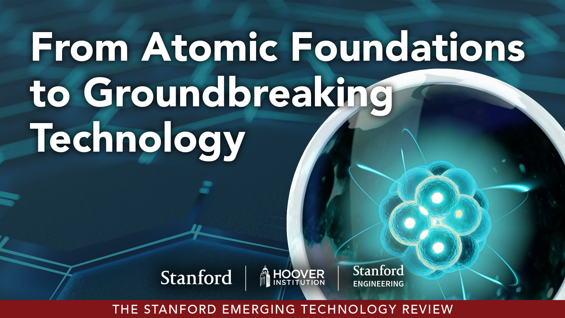
- Material science studies and manipulates the structure of matter from microscopic states to macroscopic states molecules and atoms to large objects. It enables groundbreaking advances in fields like semiconductors, energy, robotics, space exploration, and biomedical technology. Star Trek imagined the future of material science with the replicator, a limitless 3D printer that can assemble atomic structures on demand while science is catching up with science fiction. Today's material science focuses on the ability to manipulate properties and relationships between atoms and molecules to create new objects with specific strengths, weights, or electrical behaviors. Lighter aircraft, batteries that can be easily recycled and safer, more effective biomedical implants. Advances in material science require an understanding of atomic structures, prediction and modeling of their properties, synthesis of new and desirable material with those properties, and manufacturing enough of it for practical applications. With this approach, researchers are already developing sustainable and recyclable plastics and smart bandages that use integrated sensors and electrical stimulation to accelerate healing wounds. Electrical circuits woven into flexible conductive materials will allow for bendable electronics changing how we design all sorts of consumer goods, from foldable, rollable, and expandable screens to biocompatible probes. For brain machine interface. Artificial intelligence can help predict and create new materials based on existing ones regulating materials that can change properties shape or size, raises concerns about the balance between public safety and innovation. Nanoparticles could offer breakthroughs in medicine and electronics, but their small size allows them to bypass biological barriers, raising questions and concerns about their ability to biodegrade safely in the body or in the environment. Future advances in applications will depend on regulatory, legal, and policy considerations. Engineering matter at the atomic level may help define the next century. How it is defined requires both innovation and regulation to ensure that microscopic mastery leads to a safe and sustainable macroscopic future.
It is a wide field. At Stanford University, for example, faculty working on materials science research programs are found in many departments, including materials science and engineering, chemical engineering, electrical engineering, bioengineering, chemistry, and physics.
Some interesting present-day applications of materials science include:
- Flexible or stretchable electronics, which involves the creation of electrical devices that can bend, stretch, and deform without compromising their performance. Such electronics can be used as wearable, skinlike devices.
- Additive manufacturing, one of the most promising advances in materials processing over the past fifteen years. Additive manufacturing, colloquially known as 3-D printing, requires several components to perform in concert, including the material resin, the light source, and the build platform where an object is printed.
- Nanotechnology is a large subfield of materials science. In the past thirty-five years, nanoscience and nanotechnology have attracted enormous interest because the properties of nanoscale materials— including their electronic, optical, magnetic, thermal, and mechanical properties—are often very different from the same material in bulk form. The unique properties of nanomaterials have enabled breakthrough applications across numerous fields, from medicine to electronics.
- Electrochemistry studies how electrical energy and chemical reactions interact through electron transfer, typically at electrode-electrolyte interfaces. Electrochemical devices can generate electrical energy through a spontaneous chemical reaction—batteries are a typical example—or they can use electrical energy to drive a chemical reaction.
- In biosensing, electrochemistry enables the detection of biological molecules—such as metabolites, hormones, and therapeutic agents—through the use of electrical signals. The high sensitivity, low cost, and portability of electrochemical biosensors, such as wearable glucose sensors for managing diabetes, make them ideal for medical diagnostics, environmental monitoring, and pathogen detection.
Look into the future
Advancements in materials science are revolutionizing how we repair, restore, and augment the human body. From supporting regenerative medicine to brain–machine interfaces, engineered materials are enabling technologies once thought to be science fiction. Prosthetics and bionics have made major leaps, thanks to high-performance materials. Lightweight composites like carbon fiber and shape memory alloys allow artificial limbs to move naturally and respond dynamically. Electrically conductive and biocompatible polymers help to form soft bioelectronic interfaces that are powering neuroprosthetics. These prosthetics aim to restore and enhance motor and sensory function by connecting directly with the nervous system.
A particularly exciting frontier is brain–machine interfaces, which depend on materials that are both biocompatible and capable of recording or stimulating neural activity. Pliant, ultrathin electrodes made from composite materials, such as flexible polymers embedded with 2-D conductors like graphene, carbon nanotubes, and metal nanowires, are designed to conform to the brain’s surface without damaging tissue. These materials interface seamlessly with neurons and can detect and decode brain signals with high resolution. This, in turn, enables the execution of computer tasks and the control of robotic limbs, providing a means of communication for paralyzed patients.
While scientists improve brain–machine interfaces for neural activity decoding, the next goal is active neuromodulation, or the ability to control neural activity with an implanted device. Currently, deep-brain neuromodulatory devices are being used to successfully mitigate symptoms of Parkinson’s disease. Researchers are also working with them to affect mood and memory. Such advances suggest that our ability to engineer materials is enabling the construction of devices that are fundamentally expanding what the human body and mind can do.
Metamaterials are artificially engineered materials with optical or acoustic properties not found in nature. These properties arise from arranging engineered microscopic structural components in particular patterns, with feature sizes smaller than the wavelength of light or sound that is of interest. The internal structure of metamaterials enables extraordinary manipulation of electromagnetic or acoustic waves, including bending them in previously impossible ways, opening new possibilities for controlling light or sound. In recent years, the field has shifted from proof-of-concept demonstrations to various applications. These include:
- Invisibility cloaks: Bending light around objects to render them nearly invisible to the naked eye.
- Superlenses: Imaging with resolution beyond the diffraction limit in microscopes and medical imaging.
- Advanced radio antennas: Compact, efficient antennas with improved signal strength for communications.
- Seismic protection: Shielding buildings from earthquakes by redirecting seismic waves.
- Acoustic control: Improved materials for sound insulation, muffling vibrations, or sound filtering in medical and industrial settings.
In the future, new applications in telecommunications, biomedicine, and energy are expected. Metamaterials are also well positioned as a foundational technology for next-generation systems from quantum computing to autonomous sensing.
Making the leap
Today’s materials science research infrastructure does not adequately support the transition from research to real-world applications at scale. Such transitions generally require construction of a small-scale pilot project to demonstrate the feasibility of potential large-scale manufacturing. At this point, the technology is too mature to qualify for most research funding—because basic science does not address issues related to scaling up—but not mature enough to be commercialized by actual companies.
Neither government funders nor venture-capital investors are particularly enthusiastic about financing pilot projects, given the significant upfront investment needed. Therefore, different forms of funding are required to bridge the gap between bench-scale research and company-level investment. Although the US government does occasionally support pilot projects, additional support in this area could also establish national rapid-prototyping centers where academic researchers can find the help and tools necessary to build prototypes and pilot plants for their technology.
Today’s research processes are also ill-suited to rapid transitions to real-world applications. The standard process has been to characterize a material and then proceed to a simple demonstration of how it might be used. Today, addressing big societal challenges calls for a more scalable, system-level approach that involves extensive rapid prototyping and fast, reliable demonstrations to provide feedback on the potential value of specific materials and to fill in knowledge gaps.
Current research arrangements make this difficult.
As with other areas of technology, materials science faces concerns about the appropriate regulatory balance between the need to ensure public safety and the imperative to innovate quickly and leapfrog possible competitors. Nanoparticles raise particular concerns because their small size may enable them to pass through various biological borders, such as cell membranes or the blood–brain barrier, potentially harming biological systems.
Collaborators and competitors
Historically, the United States has led the world in nanotechnology, but the gap between it and China has narrowed. For example, in 2024, China’s output of publications in nanotechnology was about 5.3 times as high as that of the United States.
As great-power competition intensifies, many researchers are concerned that fundamental research in the United States could now be subject to export controls. Policy ambiguity can inadvertently hinder innovation by creating obstacles for foreign researchers wishing to contribute to work in America and by deterring international collaborations with allies and partners who are important for advancing the field.
It is essential that scholars can collaborate broadly on fundamental research at an international level so that the exchange of ideas and perspectives can foster new ways of thinking that increase the likelihood and speed of technological breakthroughs.
The United States benefits from having some of the world’s largest supercomputing resources, which are essential for developing extensive databases. However, better access to computing power is necessary for researchers in materials science to generate and analyze databases effectively. Greater access to data, including to databases that might not always be openly available to academics, is also needed.